
CHOARY
Chapter 2 Introduction to Integrated Circuit Fabrication 본문
Chapter 2 Introduction to Integrated Circuit Fabrication
송쵸쵸 2021. 3. 3. 17:33이 챕터는 semiconductor fabrication(제작)의 basic을 설명한다.
2.1 Introduction
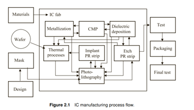
IC chip fabrication은 매우 복잡하고 시간소모적인 과정이고 이것은 IC design과 함께 시작해 EDA software의 도움으로 만들어진다.
반도체 설계업체가 설계한 칩을 파운더리 업체에 생산을 의뢰하기위해 설계와 레이아웃 과 검증을 끝내는 것을 tape out
Make shop에서, photoresist layer은 chrome glass plate위에 코팅되고 그 designed pattern은 전자빔 혹은 레이저 writer에 의해 프린트된다. PR development 이후에 chromium etch process는 mask와 reticle를 만들어 내기 위해 PR pattern을 chrome glass로 전달하기 위해 사용된다
IC design > PR layer가 chrome glass plate위에 코딩됨 > design된 pattern이 전자빔이나 레이저에 의해 프린팅됨 >chromium etch process> cleaning/inspectrion
Rough silicon from quartz sand > purify the silicon > pull it into a single-crystal ingot > slice the ingot into wafer > wet etching > surface polishing > go to the semiconductor fabs
Cleaned > thermal processed, photolithography , etch , ion implantation , dielectric thin-film deposition , chemical mechanical polishing >> go to a testing and packaging house
Wafer는 항상 cleanroom에서 유지됨
2.2 Yield
Yield는 IC fabrication의 가장 중요한 요소 중 하나임.
Yield는 environment, material, equipment, processes 등에 관련되어 있음
Yield를 향상시키는 것은 IC fab들에서 항상 yield engineer들을 고용하는 매우 필수적인 요인이다.
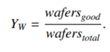
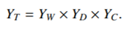
IC chip fabrication안에는 3가지 다른 yield가 있다 / wafer yield, Die yield, Packaging yield
Wafer yield
Die yield

Packaging yield

Wafer yield는 대부분 processing과 wafer handling과 관련되어있다.
Careless human wafer handling, robot malfunction, and robot miscalibration can break the brittle silicon wafers. Incorrect processing, such as misaligned photolithography followed by etch or ion implantation, wrong dopant concentration, nonuniformity of film thickness in thin-film deposition, large amounts of particles on a wafer, etc.,
Die yield는 particle contamination, process maintenance, total processing steps 등과 관련되어 있다.
Overall yield는 이 세 가지 yield를 모두 곱한 값으로 매우 중요하다.
2.2.2 Yield and profit margin
Yield가 왜 이렇게 중요한지 예시
The cost of a 300-mm wafer varies from time to time, mainly determined by the condition of supply and demand. Depending on circuit requirements, a wafer requires several-hundred processing steps before it can be sent to a packaging house to be tested and packaged. Each processing step adds some cost, typically about $1 USD per wafer. If we assume a wafer costs $200, and it takes 500 steps to complete the processing, the total cost per processed wafer is $200 (wafer cost) + $500 (processing cost) = $700. We can assume 100% wafer yield, which means no wafer scrap during the 500 processing steps. We can also assume the cost of test and package for each good die is $10, and no dies failed during final testing after package completion (100% packaging yield). In the case of 500 chips per wafer, and each chip selling for $30, 35 good dies per wafer or a 7% die yield is needed to achieve breakeven. This can be expressed as:
$700 (wafer and processing costs) + 35 (good dies) × $10 (test and package cost) = $1050 = 35 (good dies) × $30 (revenue/die).
$700 (wafer and processing costs) + 35 (good dies) × $10 (test and package cost) = $1050 = 35 (good dies) × $30 (revenue/die). If the die yield increases to 50% while wafer yield and package yield both stay at 100%, the total cost per wafer will be $700 (wafer and processing cost) + 250 × $10 (test and packaging cost) = $3200, while the revenue per wafer will be 250 × $30 = $7500. The profit margin per wafer is $7500 − $3200 = $4300. This means that if a wafer fab can process 10,000 wafers a month with 100% wafer yield, 50% die yield, and 100% packaging yield, it can make $43 million in profit a month
Yield의 문제는 몇 예상할 수 없는 processing equipment,human error의 문제에 의해 발생한다.
2.2.3 Defects and yield
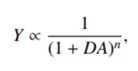
Ø Y : overall yield , D : killer defect density, A : chip area n : the number of processing steps
이 방정식으로부터 우리는 D(killer defect density)가 거의 0에 수렴해야 100%의 Yield를 달성할 수 있음을 알 수 있다.
몇몇 production wafer들은 several test dies와 함께 디자인된다
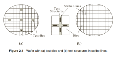
기술 향상으로 인해 die들 사이의 scribe line위에 만들어진다.
2.3 Cleanroom Basics
아주 작은 particle들도 microelectronic device와 circuit에 영향을 미치고 이것은 chip yield에 영향을 주기 때문에 IC chip들은 cleanroom안에서 다루어 져야 한다.’
A smaller feature size requires a higher grade of cleanliness in the cleanroom.
더 feature size(the size of the elements on a chip)가 작아질수록 a higher grade of cleanliness in the cleanroom이 필요 되어진다.
2.3.1 Definition of a cleanroom
A cleanroom is a manmade minienvironment that has much lower particle counts than the normal environment.
Cleanroom은 일반적인 환경보다 much lower particle을 가진 인공적인 minienvironment이다
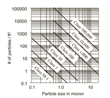
The standard definition of cleanroom class is a strange combination of metric and English units: class 10 is defined as less than 10 particles with diameters larger than 0.5 µm per cubic foot. Class 1 is defined as less than 1 particle with diameters larger than 0.5 µm per cubic foot.
Class 1 , class 10, class 100 이런 식으로 기준이 나뉘어져 있음
2.3.2 Contamination control and yield
Particles on a wafer can cause defects, which can reduce yield and affect the profitability of an IC fab.
웨이퍼 위에 있는 Particle들은 defect들을 유발할 수 있고 이것은 yield를 감소시키며 수익성을 감소시킨다.
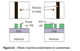
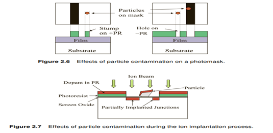
imaging of particles on the clear area of a mask or reticle can cause pinholes for negative photoresist, or stumps for positive photoresist, during photolithography processing.
Negative photoresist, Positive photoresist
During etch processing, these pinholes and stumps are transferred to the wafer surface and cause defects
Etch processing 중에, 이러한 pinholes와 stump들은 wafer surface로 전달되어지고 결합을 일으킨다.
Masks or reticles must be kept in the cleanest environment to prevent particle contamination.
Mask와 reticle의 경우 모든 wafer에 대해 작업이 이루어지기 때문에 cleanest한 환경에서 keep 되어야한다.
A particle with half the size of the technology node could be a killer particle. For example, an 11-nm particle can be a killer for a 22-nm IC chip. If a particle falls onto a critical area, it could be a killer even if it is smaller than half the size of the technology node. As feature size reduces, so does the size of the killer particle. Particles of different sizes behave quite differently; therefore, cleanrooms of different classes need different design concepts and require different protocols.
For example, large particles (>1 µm in diameter) can be blown away with highpressure airflow, while smaller particles cannot. Therefore, high-pressure air or nitrogen blowers are widely used in older, 100-mm (4-in.) fabs, and they are seldom used in the advanced 300-mm fabs. An air blower can remove large particles from a wafer surface; however, it adds more small particles to it.
2.3.3 Basic cleanroom structure
To cut costs, only equipment interfaces are designated as the highest class of cleanroom (where wafers are loaded into processing or metrology equipment), while fabs are built with lower-class cleanroom designs, and most facilities are installed in a subfab beneath the cleanroom floor.
Wafers are carried inside a sealed FOUP and are only exposed to airflow in the processing or metrology equipment.
웨이퍼들은 밀봉된 sealed FOUP안에 담겨 운반되어지며, processing,metrology equipment안에서의 airflow들에만 노출되어진다.
그러기 때문에 process area가 존재하지 않는다.
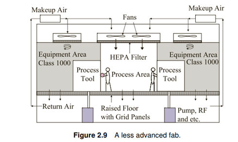
wafers are carried in an open cassette inside a carrier box. Because wafers will be exposed to airflow before they are loaded into the processing or metrology equipment in an open cassette, the wafer processing areas are designed as a high-class cleanroom.
The wafer processing area들은 high-class cleanroom으로 제작되어졌다.
To achieve better than class-100 cleanliness, it is very important to keep a linear airflow, usually called laminar flow, and avoid air turbulence.
Turbulence 난기류
Air turbulence can drive out particles sticking to the surfaces of walls, ceilings, tables, and tools, causing them to become airborne, and helps these particles stay airborne for a longer time, increasing the number of particles in the air.
A cleanroom is always kept at a higher pressure than nonclean areas; this allows continual outward airflow, preventing the entry of airborne particles from the outside when a door is opened to let people, tools, or other materials enter the cleanroom.
Cleanroom은 항상 nonclean area들보다 높은 압력으로 유지된다. 이것은 continual한 outward airflow들을 유지하며 문이 열릴 때 밖으로부터 오는 airborne particle들이 들어오는 것을 방지한다.
temperature, airflow rate, and humidity are strictly controlled in the cleanroom.
나만의 요약 : 발달한 fab과 덜 발달한 fab의 차이점
Linear airflow의 중요성, Air turbulence는 각종 표면에 있는 particles을 ariborne되게 g람
Fab이 high pressure를 가지는 이유 > 그래야만 문이 열릴 때 밖에 있는 particle이 들어오지 못함
Temperature,airflow rate, humidity는 paticle들을 방해할 수 있으며 airborne 상태를 유발시킬 수 있음
2.3.4 Basic cleanroom gowning procedures
Therefore, people working inside the cleanroom must wear specially designed garments. Because people are the main contamination sources, some companies have even limited the number of people working in the cleanroom to control contamination.
Improvement of cleanroom garments and strict cleanroom gowning procedures have sharply reduced contamination from people working inside the cleanroom.
Cleanroom 의복들과 엄격한 cleanroom gowning procedure들의 improvement들은 cleanroom안에서 일하는 사람들로부터의 contamination을 빠르게 제거해갔다.
2.3.5 Basic cleanroom protocols
While cleanroom protocols are different from company to company, the basic concepts are the same: keeping particles where they are and not letting them become airborne, and preventing other contaminants from reaching the wafers.
회사마사 cleanroom protocol들이 다르긴 하지만 기본적인 concept들은 같다. / particle들이 안으로 들어오는 것을 막고 그들이 airborne 상태가 되는 것을 막으며 결국 그 들이 wafer들에 도달하는 것을 prevent하는 것이다.
2.4 Basic Structure of an Integrated Circuit Fabrication Facility
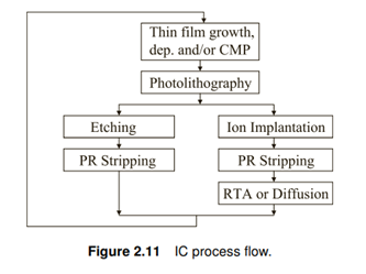
Semiconductor manufacturing has many different processes, which can be characterized by the following four basic operations: adding, removing, patterning, and heating. Doping, layer growth, and deposition are adding processes;
Semiconductor manufacturing은 많은 different process들을 가지고 있다. 이 과정들은 adding,removing,patterning,heating으로 이루어져있으며, Doping,layer growth, deposition은 추가적인 process들이다.
etch, clean, and polish are removing processes; photolithography is the patterning process; and annealing, alloying, and reflow are the heating processes.
Etch,clean,polish = removing processes.
Photolithography = patterning processes.
Annealing, alloying, reflow = heating processes.
Wafer processing, equipment, chip testing areas, and packaging are located in a cleanroom, while other areas such as offices, facilities, and processmaterials storage are located elsewhere on site.
나만의 요약 :
Etch,clean,polish = removing processes.
Photolithography = patterning processes.
Annealing, alloying, reflow = heating processes.
Wafer processing, equipment, chip testing areas, packaging은 cleanroom에 위치 되어있음.
Wafer들은 항상 highest class의 클린룸에 위치함
많은 수의 processing equipment들은 더 낮은 class의 cleanroom에 위치되있고 그 지역을 gray area라고 부름
Chip testing and packaging은 그것보다 너 낮은 class의 cleanroom에 위치함
2.4.1 Wafer processing area
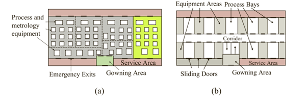
Wafer processing areas are usually separated into several processing areas, or bays, as shown in Fig. 2.12.
. They are: the wet bay, diffusion bay, photo bay, etch bay, diffusion bay, thin-film bay, and chemical mechanical polishing (CMP) bay.
Wafer processing area들은 항상 몇몇 processing area들로 분리되어 있다.
2.4.1.1 Wet bay
The wet bay is where wet processes take place.
Wet bay는 wet process들이 이루어지는 place이다.
Photoresist stripping, wet etching, and wet chemical clean processes are the most common processes in the wet bay.
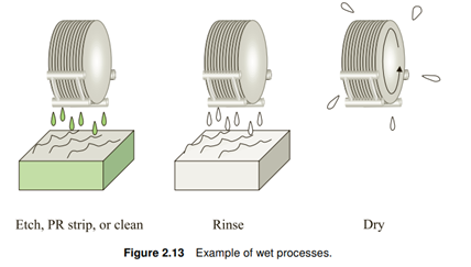
Robots take the cassette with wafers from the loading station and dip it into a processing solution. After the required process time, robots pick the cassette up and put it into a rinse sink, where DI water washes away the chemicals from the wafer surface. Then the cassette is picked up and sent into a dryer, where wafers are spun dry with the cassette.
To reduce chemical usage, single-wafer wet processing tools have also been developed. By processing wafers one at a time, only a small amount of chemical needs to be sprayed onto the wafer surface; thus, the amount of chemical used in the wet process can be significantly reduced in comparison to the batch system, in which the whole cassette is submerged in the wet chemical. Some fabs do not have a separate wet bay; wet chemical st
화학 물질 사용량을 줄이기 위해 단일 웨이퍼 습식 처리 도구도 사용되었음
웨이퍼를 한 번에 하나씩 처리하여 소량의 약품 만 웨이퍼 표면에 뿌려기 때문에 따라서 사용되는 화학 물질의 양을 배치 시스템에 비해 크게 줄일 수 있음
2.4.1.2 Diffusion bay
The diffusion bay is where thermal processes are performed.
Diffusion bay는 thermal process가 이루어지는 place이다.
These processes can be adding processes, such as oxidation, low-pressure chemical vapor deposition (LPCVD), and diffusion doping, or heating processes, such as postimplantation annealing, dopant drive-in, alloy annealing, and dielectric reflow.
These process들은 oxidation, low-pressure chemical vapor deposition(LPCVD), diffusion doping, heating processes와 같은 processes이다.
2.4.1.3 Photo bay
The photolithography process is one of the most important processes in IC fabrication.
Photolithography process는 IC fabication에서 가장 중요한 process이다.
It transfers the designed pattern from a mask or reticle to the photoresist coated onto the wafer surface.
이것은 mask나 reticle로부터 wafer 표면에 coated 되어있는 photoresist에 designed된 pattern을 전달한다.
In the photo bay are located the integrated track-stepper systems, which perform primer and photoresist coating, baking, alignment and exposure, and photoresist development processing steps.
Photo bay안에는 primer and photoresist coating, baking, alignment and exposure, and photoresist development processing steps을 형성하는 통합 track-stepper system들이 위치하고 있다.
A stepper is the most commonly used tool to pattern the photoresist coated onto the wafer surface by exposing the photoresist to ultraviolet (UV) light or deep UV (DUV) light, thereby inducing photochemical reactions.
Stepper는 photoresist를 UV light 나 DUV light에 노출시킴으로써 wafer 표면에 코팅된 photoresist를 pattern하는데에 가장 공용으로 사용되는 tool이다.
There are also optical microscopes for visual inspection, and scatterometry systems for CD measurements
또한 CD 측정을 위한 visual inspection, scatteromerty를 위한 optical microscope들이 있다.
2.4.1.4 Etch bay
After the photoresist is patterned and passes inspection, the wafers are sent either to the implant bay or to the etch bay
Photoresist가 patterned되고 점검된 후 wafer들은 implant bay 혹은 etch bay로 보내진다.
In an etch bay, patterns are etched based on the pattern defined by the photoresist, permanently transferring the designed pattern to the layer on the wafer surface
Etch bay안에서, patterned들은 photoresist에 의해 정해진 pattern에 based되어 etch되고 영구적으로 wafer surface위로 designed된 pattern이 전달된다.
Etching is a removal process in which materials on the wafer surface are selectively removed chemically, physically, or most commonly by a combination of both, to create patterns on the wafer surface
Etching은 wafer surface에 pattern들을 만들기 위해서 wafer surface에 있는 material들을 chemically, physically, or most commonly by a combination of both으로 selectively하게 제거하는 removal process이다.
2.4.1.5 Implant bay
the implant bay is the only other place wafers are sent after the photolithography process.
Ion implantation and rapid thermal annealing (RTA) systems can be found in this bay.
Ion implantation is an adding process in which dopant is added to the semiconductor substrate to change its conductivity.
Ion implantation은 conductivity를 변경할 수 있는 semiconductor substrate에 dopant를 추가하는 과정임
RTA is a heating process that repairs lattice damage of the substrate at high temperatures while neither removing nor adding materials to the wafer surface.
RTA는 wafer surface에 물질을 제거하거나 추가하지 않지만 높은 온도에서 substrate의 lattice damage를 repair하는 heating process이다.
2.4.1.6 Thin-film bay
The main processes performed in the thin-film bay are dielectric and metal thinfilm deposition for interconnection applications.
2.4.2 Equipment area
Many processing tools such as ion implanters, plasma etchers, CVD reactors, and PVD and CMP tools are located in gray areas of a fab, which are cleanrooms with higher airborne particle counts, or lower-class cleanrooms, typically at class 1000.
ion implanters, plasma etchers, CVD reactors, and PVD and CMP tools 와 같은 processing 많은 tool들이 fab의 gray area들에 위치 되어있다. Gray area는 전형적으로 class 1000과 같은 낮은 class의 cleanroom을 이야기한다. 이유는 가격 때문이다.
2.4.3 Facility area
The facility area hosts facilities that support the processing tools and metrology instruments.
Facility area는 processing tools와 metrology instrument들을 support하는 facility들로 구성되어있다. 이것은 cleanroom안에 위치하지 않았고 같은 건물이 아닌 경우도 종종 있다.
Facilities needed for the wafer processes are gases, water, electric power, and subsystems that support the processing equipment.
'SEMICONDUTOR > Book summary' 카테고리의 다른 글
| 3.1.1 Bandgap (0) | 2021.08.02 |
|---|---|
| Chapter 3 59P [부제: 시작이 반이다] (0) | 2021.08.01 |
| Introduction to Semiconductor Manufacturing Technology Chapter 1 Introduction (0) | 2021.02.17 |


